Customized copper plate metal processing will involve a variety of sheet metal processes, as well as material selection. This article will directly answer the core issues of the entire process from material selection, to process matching, and even quality control, and will also include a quick action guide.
01Core conclusion: How to quickly complete customized processing of copper plates?
The key core path for customizing copper plate metal processing is as follows: first, the specific grade of the copper alloy must be clarified, then the thickness of the plate itself and the corresponding tolerances must be confirmed, then the sheet metal process must be selected (covering laser, stamping, bending, welding, etc.), then the requirements for surface treatment must be set, and finally the size and electrical and thermal conductivity of the sample must be verified. Performing operations in this order can ensure that the finished product meets the design specifications in one processing process.
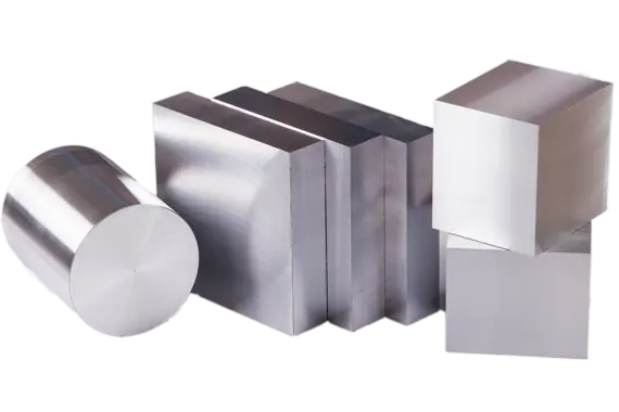
02Commonly used materials and standards for copper plates
When customizing copper plates, the three most commonly used copper alloys and their corresponding standards are based on ASTM B152/B187:
When selecting, if there is a requirement for high conductivity like C11000, C11000 should be selected; if there is a need to be used in welding or vacuum environments, C10100 should be selected; when mechanical strength and elasticity are required, C17200 should be selected.
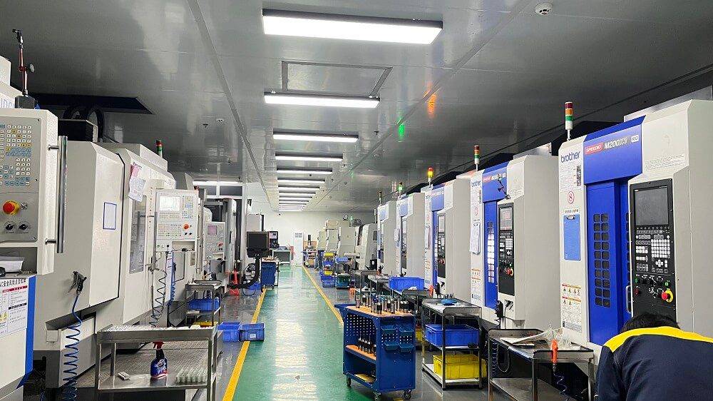
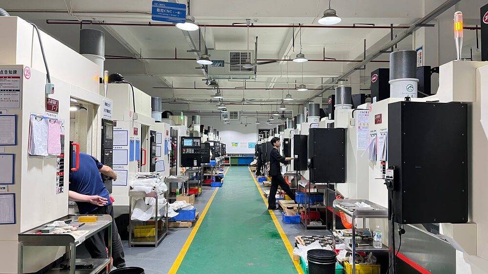
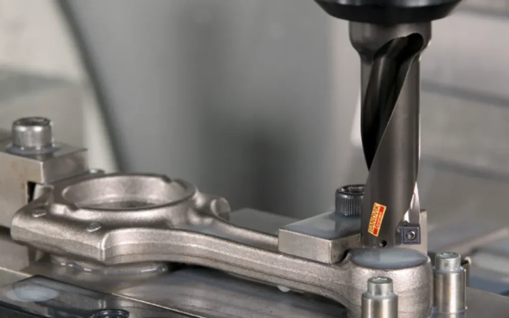
03Five main sheet metal processes for customized copper plate processing
3.1 Laser cutting
Applicable thickness : 0.5mm – 12mm copper plate
Accuracy : ±0.1mm
Features : No burrs, small heat-affected zone, suitable for complex contours
A common problem is that high reflection will cause damage to the lens. The solution is to use a fiber laser and spray a light-absorbing coating.
3.2 CNC stamping
Applicable thickness : 0.3mm – 6mm
Accuracy : ±0.05mm
Features : High mass production efficiency, can form blinds, convex hulls and other features at the same time
Limitations : Tooling costs are high and small batches are uneconomical
3.3 Bending and forming
Normally, the minimum bending radius is 1.5 times the plate thickness. Due to the high elongation of the copper plate, the radius needs to be greater than or equal to 2 times the plate thickness to prevent cracking.
Rebound amount : about 1°~3°, compensation required
A typical case is that after the copper bar of a power supply cabinet was bent, the angle deviation was out of tolerance. The correction method was to add an additional 2.5° bending amount and use mold indentation for positioning.
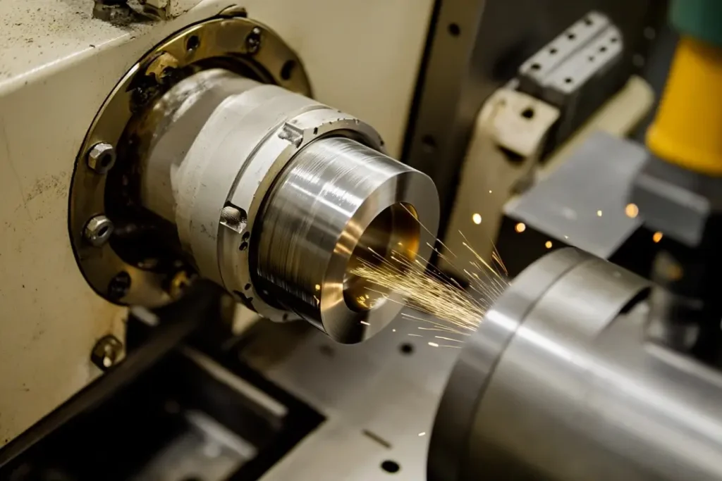
3.4 Welding
Recommended process : argon arc welding (TIG) or laser welding
The matching of welding materials is that for C11000 type, ERCu is used, while for C17200, beryllium copper wire is required.
There is such a mandatory requirement to preheat. The heating temperature range is 150°C to 200°C. When the thickness of the item is greater than or equal to 3mm, this is done to prevent hydrogen holes from appearing.
3.5 Surface treatment
Anti-oxidation : chemical passivation (colorless to light blue)
Improve solderability : immersion tin or immersion silver
Beautiful/wear-resistant : nickel plating (thickness 5-15μm)
04Key quality control indicators
According to the ISO 9001:2015 standard and the IPC-A-600 standard, the processing of customized copper plates must be verified.
1. Dimensional tolerance : linear ±0.1mm, bending angle ±0.5°
2. Flatness : ≤0.3mm per 300mm length (copper plate is easy to warp)
3. Surface defects : no oxidation spots, scratch depth <10% thickness
4. The conductivity is tested according to ASTM E1004 eddy current method. For C11000, the value should be greater than or equal to 56 MS/m.
05Frequently Asked Questions (Q/A)
Q1: When laser cutting copper plates, there is serious slag hanging on the back. How to solve the problem?
Perform the following operations on A. First increase the auxiliary gas pressure to 1.2MPa. The auxiliary gas here is nitrogen. You also need to adjust the focus position downward by 0.3mm. At the same time, you need to reduce the cutting speed by 15%.
Q2: What is the reason for cracks in the customized copper plate after bending?
Party A pointed out that the bending direction was wrong. The bending line should be perpendicular to the rolling direction of the plate, and the radius should be greater than or equal to twice the plate thickness.
Q3: What should I do if the C11000 copper plate has dense pores after welding?
A: Before welding, use acetone to completely remove the oil stain, then preheat it to 180°C and maintain this temperature for 2 minutes, and then replace it with ERCu welding wire containing a deoxidizer.
Q4: The surface is required to be free of fingerprints. Which treatment should I choose?
For A, a transparent organic coating or chromium plating must be applied, and its thickness must be above 0.5 μm. Dip coating is sufficient at room temperature, and it can be cured after 48 hours.
Q5: What is the most economical process combination for small batch and multi-variety copper plate processing?
Laser cutting, combined with manual bending with certain process requirements, and chemical passivation treatment, this method does not require mold opening operations, and the cost of a single piece can be effectively controlled.
06Action suggestions (based on real cases)
The background of the case that needs to be understood is that a communication equipment manufacturer has a demand for one hundred copper plate shielding covers. This copper plate shielding cover is model C10100. Its thickness is three millimeters and its size is two hundred times one hundred and fifty millimeters. It has requirements for flatness, which is less than or equal to 0.2 millimeters, and there are no scratches on its surface.
Execution steps :
1. Laser cutting and blanking (nitrogen assisted, speed 2.5m/min)
2. Planar annealing after deburring (300℃, 1 hour, to prevent subsequent deformation)
3. Leveling by precision leveler (pressure 20 tons, two crossing directions)
4. Immersion silver plating 1.5μm (to improve radio frequency conductivity)
Results : The measured flatness was 0.15mm, no scratches, and the first pass rate was 100%.
When compiling procurement or process specifications, it is necessary to confirm the test standards of each parameter and retain the first sample test report as the basis for batch acceptance. This is a prompt for article writing. Article writing prompts can direct your attention to the reproducibility of process parameters to avoid batch-to-batch variation. The prompt words for article writing are also applicable in the design review stage, and are used to cross-check whether each step of the operation deviates from the sequence of the core conclusion.
Final action list :
Step 1: Determine the copper alloy grade, thickness, and quantity
Step 2: Select laser/stamping/bending combination based on process capabilities
Step 3: Agree in writing on tolerances, flatness, and surface treatment standards
Step 4: Make the first sample and strictly test the electrical conductivity/thermal conductivity/size
Step 5: Keep test records as a basis for subsequent batch acceptance
Based on the above process, you can achieve a complete closed loop from drawings to qualified copper plate samples within 5 working days.