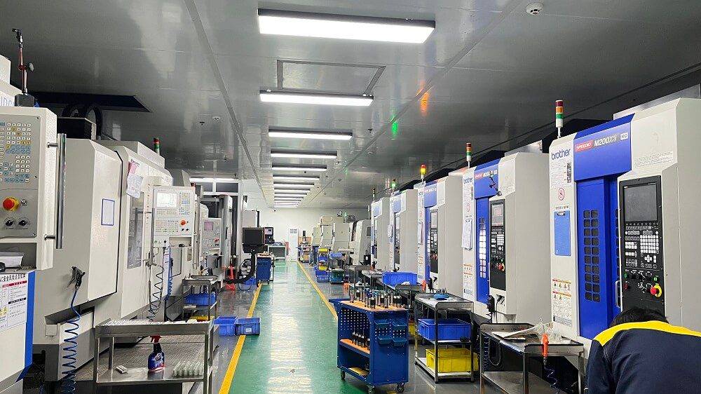
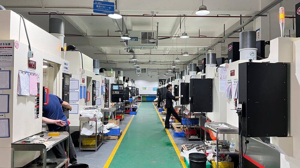
With the rapid development of the semiconductor industry, processes such as wafer fabrication, etching, coating, testing, and packaging impose extremely high demands on the precision, cleanliness, and material properties of equipment components. A large number of critical parts rely on high-precision CNC machining and precision manufacturing processes for completion.
This article systematically introduces common types of machined semiconductor parts, their processing characteristics, and commonly used materials, helping you quickly grasp the core essentials of semiconductor component machining.
I. Core Requirements for Semiconductor Machined Components
Compared to conventional industrial parts, semiconductor components typically require the following during machining:
• Ultra-high machining precision (micrometer-level or even sub-micrometer-level)
• Exceptionally high surface finish to prevent particle contamination
• Stringent cleanliness control meeting cleanroom standards
• Resistance to high temperatures, corrosion, and plasma environments
• High material stability with low outgassing and minimal impurities
Consequently, semiconductor components often necessitate a combination of precision CNC machining, grinding, polishing, surface treatment, and rigorous inspection.
II. Common Types of Machined Semiconductor Components
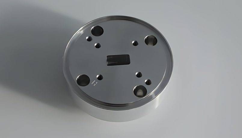
1. Wafer Chuck
Function: Secures and supports wafers, maintaining stability during processes such as lithography, etching, and inspection.
Machining Characteristics:
• Extremely high flatness and parallelism
• Surface requires precision grinding or polishing
• Prevents wafer slippage or deformation
Common Materials:
• Aluminum alloy
• Stainless steel
• Ceramics (aluminum oxide, aluminum nitride)
2. Photomask
Function: Used in photolithography to transfer circuit patterns onto wafer surfaces.
Machining Characteristics:
• Extremely high pattern precision
• Strict cleanliness requirements
• Typically combines precision machining with photolithography
Common Materials:
• Quartz glass
• Chromium-plated film
3. Probe Card
Function: Enables electrical signal contact during wafer testing.
Processing Characteristics:
• Micro-structure machining
• High-precision positioning
• Excellent electrical conductivity
Common Materials:
• Silicon
• Ceramics
• Precious metals (e.g., gold, platinum)
4. Annealing Furnace Components
Function: Used for high-temperature thermal processing of wafers.
Processing Characteristics:
• High-temperature resistance, thermal shock resistance
• Chemical corrosion resistance
• Requires structural stability
Common Materials:
• Quartz
• Ceramics
• High-temperature alloys
5. Etching Equipment Parts
Function: Used in plasma etching and wet etching equipment.
Processing Characteristics:
• Complex geometric structures
• Resistance to highly corrosive gases and chemical media
• Special surface treatment required to extend service life
Common Materials:
• Fluoroplastics such as PTFE, PFA
• Stainless steel
• Ceramics
6. Deposition Equipment Components
Function: Used in CVD, PVD, and other thin-film deposition processes.
Processing Characteristics:
• Suitable for high-vacuum environments
• High surface finish
• Low impurity levels, low outgassing
Common Materials:
• Stainless steel
• Aluminum alloys
• Titanium alloys
7. Transfer Arm
Function: Transports wafers or workpieces within equipment.
Processing Characteristics:
• Lightweight design
• High rigidity and repeatability
• Typically requires precision assembly and dynamic debugging
Common Materials:
• Aluminum alloy
• Carbon fiber composite
8. Packaging Mold
Function: Used for semiconductor packaging molding.
Processing Characteristics:
• Complex cavity structure
• High hardness and wear resistance
• Combination of precision mold machining and heat treatment
Common Materials:
• Tool steel
• Cemented carbide
9. Cleaning Bath
Function: Used for chemical cleaning of wafers or components.
Processing Characteristics:
• Extremely high cleanliness
• Resistance to strong acid/alkali corrosion
• Internal surfaces require fine polishing
Common Materials:
• Stainless steel
• High-purity quartz
III. Key Technologies for Machining Semiconductor Components
Manufacturing semiconductor equipment components typically requires integrating the following processes:
• High-precision CNC turning/milling
• Precision grinding and mirror polishing
• Special surface treatments (anodizing, spraying, plating)
• Ultrasonic cleaning and clean packaging
• Rigorous dimensional and cleanliness inspection
Each process step directly impacts the stability, lifespan, and yield of components within semiconductor equipment.
IV. Conclusion
Semiconductor machined components form the critical foundation supporting the entire chip manufacturing process. From wafer fixtures to etching, coating, and packaging equipment components, each part demands exceptionally high standards for precision, materials, and manufacturing processes.
Selecting manufacturers with precision CNC machining capabilities, semiconductor industry expertise, and rigorous quality control systems is essential for ensuring the long-term stable operation of semiconductor equipment.