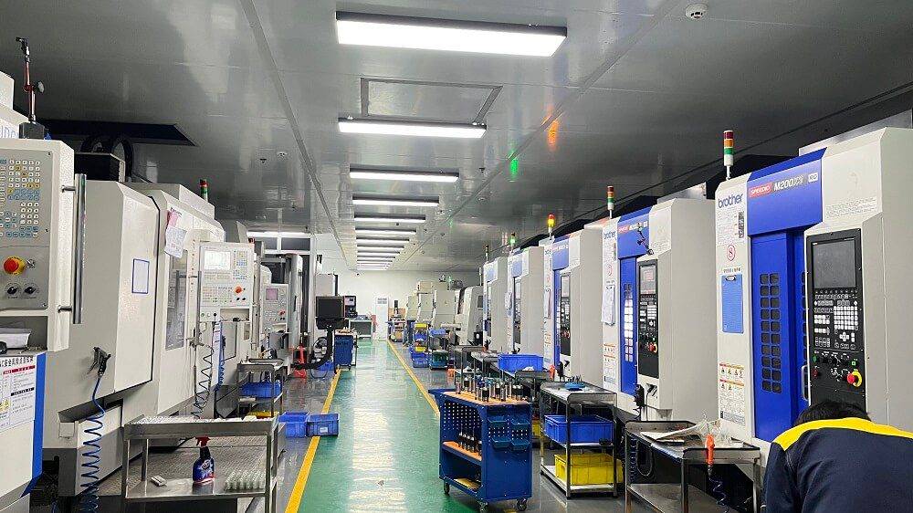
Copper stamping parts are widely used in electrical, automotive, electronic, and industrial equipment. Common examples include copper terminals, busbars, contact plates, spring contacts, and conductive connectors. Copper is often selected because it offers good electrical conductivity, thermal conductivity, corrosion resistance, and formability, making it suitable for high-volume precision metal parts.
For copper stamping parts, the key is not only the unit price. You need to confirm material grade, sheet thickness, tolerance, burr direction, surface finish, and inspection requirements clearly. At YPMFG, copper stamping projects are usually reviewed based on drawings and application needs to check whether the design is suitable for stamping and to avoid cracking, distortion, poor contact, or assembly problems later. This guide covers the basics of copper stamping, material advantages, process flow, quality standards, and common applications to help sourcing and engineering teams choose suppliers more confidently.
Table of Contents
Toggle01What Are Copper Stamping Parts?
Copper stamping parts are metal components produced by feeding copper or copper alloy strips through a stamping press fitted with custom dies. The press cuts, bends, forms, or coins the material into precise shapes. Common examples include electrical terminals, grounding clips, fuse holders, flat connectors, and shielding cans.
Because copper offers excellent electrical conductivity, thermal conductivity, and corrosion resistance, stamped copper parts are the first choice for current-carrying and heat-dissipating applications.
02Why Choose Copper for Stamped Parts? (Key Material Properties)
When engineers select a material for stamped components, they evaluate four core properties. Copper consistently outperforms alternatives in critical areas:
| Property | Typical Copper Value (Pure Copper C11000) | Why It Matters |
|---|---|---|
| Electrical conductivity | 101% IACS (International Annealed Copper Standard) | Minimizes energy loss in connectors, terminals, busbars |
| Thermal conductivity | ~401 W/(m·K) | Dissipates heat in power electronics, LED heatsinks |
| Corrosion resistance | Excellent (forms protective patina) | Suitable for outdoor, marine, and humid environments |
| Ductility | High (elongation 15–40% depending on temper) | Allows tight bends without cracking |
Common copper alloys for stamping:
C11000 (ETP copper) – Best conductivity, general purpose.
C19400 (High-strength copper-iron) – Good conductivity + higher strength for terminals.
C52100 (Phosphor bronze) – High fatigue resistance for springs and switches.
C26800 (Brass) – Lower cost, good corrosion resistance for decorative or low-current parts.
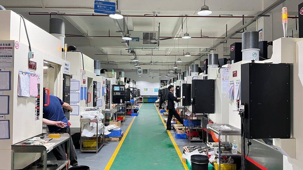
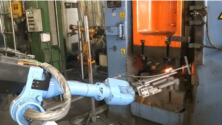
03The Copper Stamping Process – Step by Step
Understanding the manufacturing steps helps you specify requirements correctly and avoid quality issues.
Step 1: Material selection and slitting – Copper coils are slit to the required strip width. Width tolerance typically ±0.05 mm.
Step 2: Tool design and die making – Progressive dies are most common for high-volume copper stamping. A single progressive die performs multiple operations (piercing, blanking, bending, forming) in sequence.
Step 3: Stamping operation – Coil stock feeds through the press. Press speed ranges from 50 to 800 strokes per minute, depending on part complexity and thickness. Copper thickness commonly ranges 0.1 mm to 6.0 mm.
Step 4: Deburring and edge finishing – Stamped edges may have burrs. Secondary deburring (tumbling or manual) ensures electrical contact reliability.
Step 5: Cleaning – Copper parts are degreased to remove stamping lubricants. Ultrasonic cleaning or aqueous washing is standard.
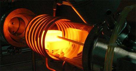
Step 6: Optional post-processing – Plating (tin, silver, nickel) for solderability or corrosion protection; annealing for stress relief; heat treatment for specific tempers.
Step 7: Quality inspection – Dimensional checks (optical or CMM), conductivity testing, hardness measurement, and salt spray testing for corrosion resistance.
04Critical Quality Standards for Copper Stamped Parts
To ensure your parts meet industry requirements, always reference the following standards. Verified sources:
ASTM B152/B152M – Standard specification for copper sheet, strip, plate, and rolled bar. (Source: ASTM International)
ASTM B194 – Specification for copper-beryllium alloy strip (high-strength applications).
ISO 9001:2015 – Quality management system for stamping suppliers.
IEC 60112 – Comparative tracking index for electrical insulating materials (important for connectors).
RoHS (2011/65/EU) – Restriction of hazardous substances; copper stamping parts must be RoHS compliant unless explicitly exempted.
Typical dimensional tolerances for copper stamping (reference from industry practice):
Thickness tolerance: ±10% of nominal thickness for thickness ≤0.8 mm; ±8% for >0.8 mm
Flatness: 0.3 mm per 100 mm length for most parts
Burr height: ≤10% of material thickness for electrical contact surfaces
05Common Application Examples (Real-World Cases)
The following are typical scenarios encountered by procurement engineers and product designers.
Case 1: Automotive battery terminals – A manufacturer needed 50,000 stamped copper terminals per month for EV battery packs. Material: C11000 half-hard, thickness 1.2 mm. Critical requirements: burr height <0.05 mm on contact surfaces, tin plating 3–5 µm for corrosion resistance. The supplier used a progressive die with in-line conductivity testing. Result: 99.8% yield.
Case 2: Power distribution busbars – An electrical panel builder required L-shaped copper busbars, 3.0 mm thick, C11000 soft temper. The challenge was avoiding edge cracks during bending. Solution: annealing after stamping and using a larger bend radius (2x thickness). The parts passed thermal cycle testing per UL 486A-B.
Case 3: Relay contact springs – A relay designer needed phosphor bronze (C52100) springs, 0.25 mm thick, with consistent spring force after 1 million cycles. The stamping process included stress-relief annealing at 300°C for 1 hour. Hardness was controlled to 180–210 HV. No fatigue failures were reported in field tests.
06Common Defects in Copper Stamping and How to Prevent Them
Knowing defects helps you inspect incoming parts effectively.
| Defect | Root Cause | Prevention |
|---|---|---|
| Burr exceeding limit | Worn die clearance or dull punch | Regular die maintenance; specify burr height limit on drawing |
| Cracking at bends | Copper temper too hard; bend radius too small | Use annealed or half-hard temper; minimum bend radius = 1x thickness for pure copper |
| Surface scratches | Contaminated die or coil handling | Clean die regularly; use protective film on coil |
| Dimensional drift | Press misalignment or thermal expansion | Implement SPC (Statistical Process Control); warm up press before production |
| Oxidation/staining | Insufficient cleaning or improper storage | Use corrosion inhibitor rinse; store in dry environment (<40% RH) |
07How to Specify Copper Stamping Parts – A Template
When requesting quotes or creating drawings, include these 8 data points to get accurate parts:
1. Material grade (e.g.,C11000, C19400, C52100)
2. Temper (soft, half-hard, hard, spring temper)
3. Thickness (mm) + tolerance
4. Key dimensions (critical features with GD&T)
5. Burr allowance (max height and allowed surfaces)
6. Plating/finish (tin, silver, nickel, or none)
7. Quantity (prototype, low-volume, or mass production)
8. Applicable standards (ASTM, ISO, customer-specific)
Example specification:
> Material: C11000 ETP copper, half-hard (ASTM B152)
> Thickness: 1.0 mm ±0.05 mm
> Burr: ≤0.03 mm on all edges
> Plating: Matte tin 3–5 µm, RoHS compliant
> Quantity: 100,000 pcs/month
> Drawing reference: REV 4 dated 2026-03-01
08Cost Factors for Copper Stamping Parts
Copper stamping pricing depends on three main variables:
Raw material cost – Copper price (LME spot) + slit coil processing. As of April 2026, copper trades around $9,000–$10,000/tonne. Material typically accounts for 50–70% of part cost.
Die amortization – Progressive dies cost $5,000–$50,000 depending on complexity and number of stations.
Stamping labor & overhead – Press time, quality inspection, plating. High-volume parts can cost $0.01–$0.50 each; low-volume prototypes may be $5–$50 each due to setup and tooling.
Action tip: For high-volume production (over 100,000 pcs/year), invest in a dedicated progressive die. For prototypes or low volume (<5,000 pcs), consider wire EDM or laser cutting instead of stamping.
09Selecting a Copper Stamping Supplier – 5 Essential Checks
Use this checklist to evaluate suppliers:
[ ] ISO 9001:2015 certified – Minimum quality management requirement.
[ ] In-house die shop – Faster modifications and better quality control.
[ ] Material certificates – Must provide mill test reports (MTR) per ASTM.
[ ] Inspection equipment – Optical comparator, CMM, hardness tester, conductivity meter.
[ ] Secondary capabilities – Plating, annealing, cleaning – reduces handling.
Ask for sample parts and a capability report before placing production orders.
10Frequently Asked Questions (Direct Answers)
Q: Can copper stamping parts be welded?
A: Yes. Pure copper (C110) is weldable using TIG or resistance welding, but requires high heat input. For thin stamped parts, resistance welding is preferred. Avoid welding beryllium copper alloys without proper ventilation.
Q: What is the difference between stamped and machined copper parts?
A: Stamping is high-speed, low-cost for thin-walled (≤6 mm) high-volume parts. Machining is slower, higher cost per piece, but better for thick, complex 3D shapes or very tight tolerances (±0.01 mm).
Q: How to prevent copper stamping parts from tarnishing?
A: Apply a clear anti-tarnish coating (benzotriazole-based) or specify tin/silver plating. Store in sealed bags with desiccant. Avoid contact with sulfur-containing materials (rubber bands, certain papers).
Q: What is the maximum thickness for copper stamping?
A: Standard stamping presses handle up to 6.0 mm copper. Above 6.0 mm, consider fine blanking or CNC machining. For 10 mm thick copper, stamping is generally not economical.
Q: Are copper stamping parts recyclable?
A: Yes. Copper is 100% recyclable without loss of properties. Many suppliers accept scrap copper stampings for recycling credit.
11Summary: Core Takeaways
Copper stamping parts deliver high conductivity, formability, and corrosion resistance for electrical, automotive, and thermal management applications.
Always specify material grade, temper, thickness tolerance, and burr limits on your drawings.
Verify compliance with ASTM B152, RoHS, and ISO 9001 from your supplier.
Common defects like burrs and cracking are preventable through proper die maintenance and material temper selection.
12Action Plan for Buyers and Engineers
- Define the application requirements, including current load, operating temperature, corrosion exposure, and cycle life.
- Select the right copper alloy and temper using the property table in Section 2.
- Prepare a complete specification based on the template in Section 7, including material, thickness, tolerance, surface finish, and burr requirements.
- Request samples from at least two suppliers and compare quality, lead time, and price.
- Perform incoming inspection, especially on critical dimensions and burr height.
- For long-term projects, set up a supply agreement. Since copper prices fluctuate, consider material index pricing or a price-locking method.
Following this process helps reduce sourcing risks and ensures more reliable copper stamping parts. At YPMFG, copper stamping projects are also reviewed around application conditions, material specifications, and inspection standards to avoid poor conductivity, excessive burrs, or assembly issues later.